Here in this article we will see about all the LCD LED TV Panel Voltage and signal test point name and its use or we will understand how this signal work.
| Connection Name | Connection Working | Voltage |
| VGH | Positive supply | 26 to 30v |
| VGL | Negative Supply | -6 to -10v |
| VON | VON is the positive supply voltage for the CKV, CKVB, and STVP (Also called “Gate-On Supply”) | 20 to 30v |
| VOFF | VOFF is the negative supply voltage for the CKV, CKVB and STVP (Also called “Gate-Off Supply”) | -6 to -9v |
| V.COM | Common Voltage for TFT | 6 to 9v |
| VSS | Digital ground | GND |
| VDD | VDD is the logic supply input for the scan driver | |
| VCL | Negative Supply | -10 to -12v |
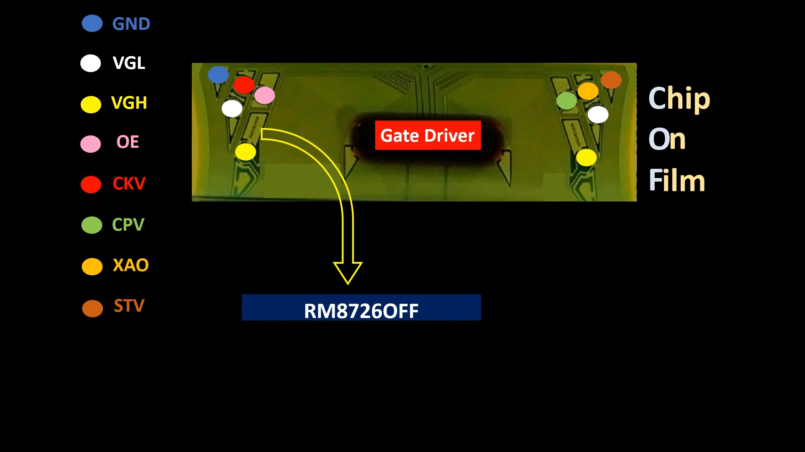
| OE (Active-High) | 1. Gate-Pulse Output Enable. 2. CKV and CKVB leave the high impedance charge-sharing state on the rising edge of OE. | Pulse/Frequency |
| STV | 1. Vertical Sync Input. 2. The rising edge of STV begins a frame of data. 3. The STV input is used to generate the high voltage STVP output. | Pulse/Frequency |
| CPV | Vertical Clock-Pulse Input. CPV controls the timing of the CKV and CKVB outputs, which change state (by first sharing charge) on its falling edge. | Pulse/Frequency |
| CKV | High-Voltage, Gate-Pulse Output. | Pulse/Frequency |
| CKVB | High-Voltage Scan-Drive Output. | Pulse/Frequency |
A Brief Details of Panel Voltage and Signal Test point Name and its use.
- OE (Active-High, Gate-Pulse Output Enable)
- CKV and CKVB leave the high impedance charge sharing state on the rising edge of OE.
- CPV (Vertical Clock-Pulse Input)
- CPV controls the timing of the CKV and CKVB outputs that change state (by first sharing charge) on its falling edge.
- STV (Vertical Sync Input)
- The rising edge of STV begins a frame of data. The STV input is used to generate the high-voltage STVP output.
- STVP (High-Voltage, Start-Pulse Output)
- STVP is low (connected to GOFF) whenever STV is low and is high (connected to GON) only when STV is high and CPV and OE are both low.
- When STV is high and either CPV or OE is high, STVP is high impedance.
- STVP High-Voltage Scan-Drive Output. STVP is connected to VOFF when STV is low and is connected to VON when STV is high and CPV1 is low. When both STV and CPV1 are high, STVP is high impedance.
- CKV (High-Voltage, Gate-Pulse Output)
- When enabled, CKV toggles between its high state (connected to GON) and its low state (connected to GOFF) on each falling edge of the CPV input. Further, CKV is high impedance whenever CPV and OE are both low and whenever CPV is low and OECON is high.
- CKVB (High-Voltage, Gate-Pulse Output)
- CKVB is high impedance to allow connection to CKV, sharing charge between the capacitive loads on these two outputs.
- CKVB is the inverse of CKV during active states and is high impedance whenever CKV is high impedance.
- CKVB1 (High-Voltage Scan-Drive Output)
- CKVB1 is the inverse of CKV1 during active states and is high impedance whenever CKV1 is high impedance.
- CKVB2 (High-Voltage Scan-Drive Output)
- CKVB2 is the inverse of CKV2 during active states and is high impedance whenever CKV2 is high impedance.
- CPV (Vertical Clock-Pulse Input)
- CPV controls the timing of the CKV and CKVB outputs, which change state (by first sharing charge) on its falling edge.
- CPV1
- CPV1 controls the timing of the CKV1 and CKVB1 outputs, which change state (by first sharing charge) on its falling edge.
- CPV2
- CPV2 controls the timing of the CKV2 and CKVB2 outputs, which change state (by first sharing charge) on its falling edge.
- SCL (Serial Clock)
- The line that carries the clock signal.
- SDA (Serial Data)
- This line is use for send and receive Data.
- VDD
- VDD is the logic supply input for the scan driver.
- VON Gate on Supply.
- VON is the positive supply voltage for the CKV, CKVB, and STVP high voltage driver outputs.
- VOFF Gate-Off Supply.
- VOFF is the negative supply voltage for the CKV, CKVB, and STVP high-voltage driver outputs.
Also Read:
WHAT IS GATE COF AND X COF PROBLEM?
COF TAB REPLACEMENT / COMPATIBLE NUMBER List